Designing an MCU/FPGA Update and Control Plane
Today, we're taking a look at Funkshun, an FPGA-based function-generator project built around an STM32F072 and a Lattice iCE40UP5K. Funkshun is still early in its development: it doesn't yet do anything you'd expect a function generator to do, like generate waveforms. What it does have is the infrastructure that makes later waveform work practical:
a cross-platform command-line interface,
field updates for both chipsets,
a safe way to share the FPGA configuration bus, and
a register protocol for communicating with the running bitstream.
Funkshun is designed as USB-controlled FPGA instrument, and is really two very different embedded systems sharing one enclosure. The microcontroller owns USB, user commands, recovery, and persistent storage. The FPGA owns the fast, deterministic datapath. They may ship as one device, but under the hood, they boot differently, fail differently, and need different tools.
Building that control plane first may look like a detour from the “real” signal-processing work. In practice, it changes the rest of the project. A new FPGA image can be built, installed, identified, and tested without moving jumpers or attaching a separate programmer. A broken image does not have to strand the device. And application registers can be exercised from a terminal before a polished UI exists.
This article walks through the design and, equally importantly, why it ended up this way.
The complete implementation is published on GitHub as lattice-spi-prog. The excerpts below are kept short so the surrounding state machines, tests, and hardware-specific code remain easy to inspect in context.
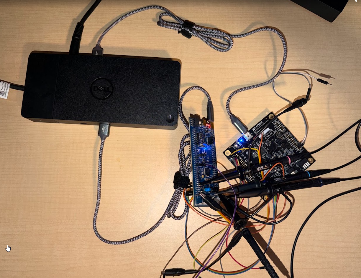
The bring-up hardware: an STM32F072 Discovery for controlling USB and updates, an iCE40 Breakout Board, and a whole mess of header jumpers and scope probes.
The Hardware
Since it's impossible to get a meaningful idea of the interconnect setup from the photo above, a short block diagram and schematic snippet can illustrate the interconnects here:
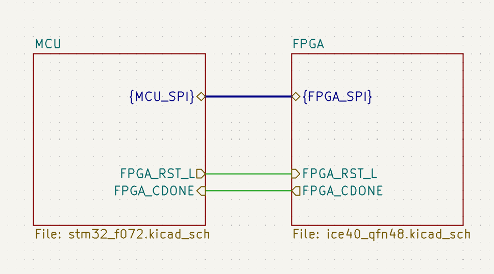
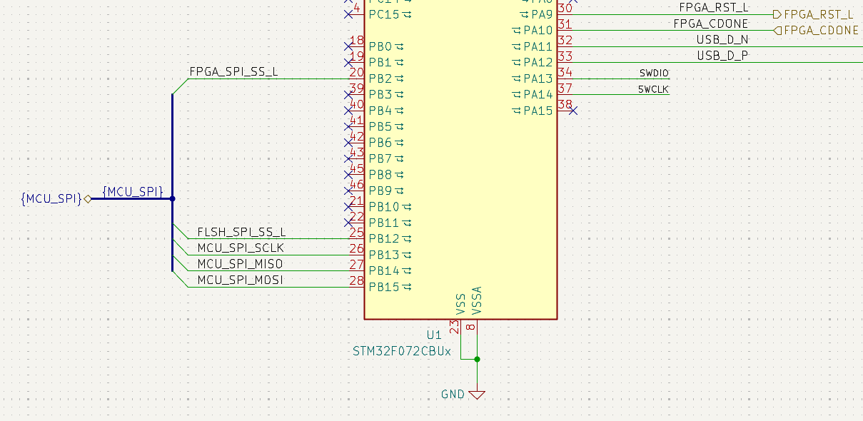
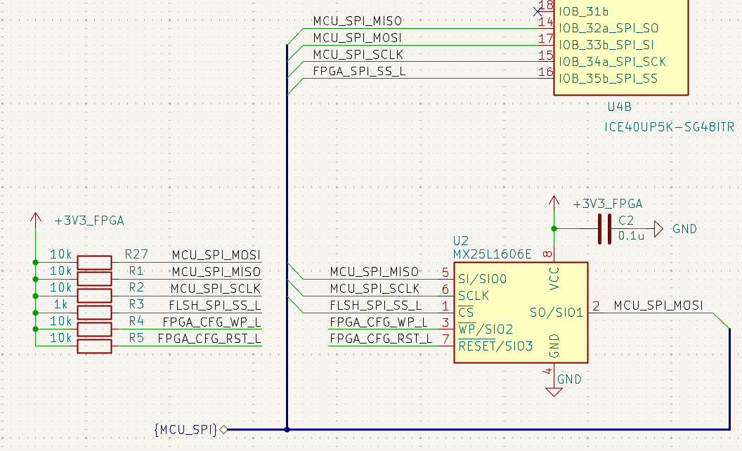
The STM32F02 implements a dual CS SPI bus, with a few additional GPIO to control FPGA_RST_L, as well as reading FPGA_CDONE. Note that the STM32 series has a ubiquitous errata whereby the SPI peripheral can't control the SS_L line directly. In this case, separate GPIO are used for controlling FPGA SS_L and SPI Flash SS_L. That's a blessing in disguise: having separate, GPIO-controlled SS_L lines allows us to share the SPI bus with multiple downstream devices, while eliminating the possibility of accessing the SPI Flash while meaning to access the FPGA. RST_L and CDONE allow the MCU to hold the FPGA in reset during flash programming, and check that the FPGA has successfully configured from the SPI bitstream.
Begin with the End User Interface
The top of the stack is fnk, a Python CLI. It presents ordinary commands instead of exposing USB endpoint details:
fnk ping
fnk info
fnk mcu update build/mcu/funkshun-mcu.bin
fnk fpga update build/fpga/funkshun-fpga.bit
fnk fpga info
fnk fpga reg-read 0x0020
fnk fpga reg-write 0x0020 0x12345678
The CLI is intentionally thin. Argument parsing and output formatting live at the edge; device behavior lives in a reusable Python API. That keeps automation from having to scrape terminal-oriented output and makes the same operations available to manufacturing fixtures, hardware tests, and future applications.
The normal USB personality is CDC ACM with a project-specific VID/PID. CDC was chosen because it is easy to inspect with existing serial tools and straightforward to support on Linux, macOS, and Windows. The apparent baud rate is only a compatibility setting - bytes travel over native USB.
The host-to-MCU protocol uses newline-terminated ASCII commands and OK or ERR responses. ASCII is not the most compact encoding, but control traffic is small, and transparency is valuable during bring-up. A terminal can send PING; a logic bug produces a readable error such as FPGA_CDONE_TIMEOUT; logs remain useful without a decoder.
That simplicity does not mean treating USB packets as messages. CDC is a byte stream. Commands can arrive fragmented across packets, and multiple commands can arrive in one packet. The MCU parser therefore accumulates text through a newline, accepts an optional carriage return, limits command text to 256 bytes, and discards an overlong command cleanly through its terminator. Tests deliberately feed fragmented and batched commands to keep packet-boundary assumptions from creeping into the firmware.
FPGA images are the exception to the ASCII rule. After a header containing the image size and SHA-256 digest, the parser enters an exact-length binary state. Every following byte—including 00, newline, carriage return, and ff—is payload until the declared count reaches zero. This two-mode protocol retains readable commands without wasting bandwidth or inventing an escaping scheme for bitstreams.
The key structure is a parser state that changes the meaning of every received byte. In binary mode, the code passes no more than the declared remainder to the image handler and switches back to command mode at exactly zero:
if (state == FNK_PROTOCOL_STATE_BINARY) {
    size_t count = length;

    if (count > binary_remaining) count = binary_remaining;

    binary_handler(data, count);
    data += count;
    length -= count;
    binary_remaining -= (uint32_t)count;

    if (binary_remaining == 0u) {
        fnk_binary_complete_handler_t complete = binary_complete_handler;
        protocol_cancel_binary();
        complete();
    }
    continue;
}
Source: protocol_feed() in mcu/src/usb/protocol.c
The host implements the complementary rule: retain partial response data between reads, scan for newline, and enforce both a deadline and a maximum line length in ProtocolClient.read_response().
Updating the MCU without maintaining a bootloader
The STM32F072 already contains an immutable USB DFU bootloader in system ROM, so Funkshun uses it rather than reserving flash for a custom bootloader. The application acknowledges MCU UPDATE, flushes that response, detaches its USB peripheral, restores a reset-like clock state, remaps system memory, installs the ROM stack pointer, and branches into the factory loader.
On the host, fnk watches the application CDC device disappear, waits for the STM32 DFU VID/PID, confirms that exactly one suitable Internal Flash target is present, invokes dfu-util, and waits for the same application USB serial number to return. It then asks the new firmware for its identity.
Those steps are represented directly in mcu.update(), rather than being hidden inside one optimistic shell command. For example, the application acknowledgement is checked before the original serial handle is closed:
emit("Entering STM32 DFU...")
acknowledgement = self._owner._client.request("MCU", "UPDATE")
if acknowledgement != "ENTERING_DFU":
    raise FirmwareUpdateError(
        f"application refused MCU update: {acknowledgement!r}"
    )

self._owner._client.close()
self._wait_for_application_absent(application.serial_number, timeout)
target = dfu.wait_for_target(timeout)
dfu.program(target, path)
This orchestration is more important than the flash command itself. USB device names can change after re-enumeration. Another DFU-capable board might already be attached. The application must not disconnect before its acknowledgement reaches the host. Every transition therefore has a bounded timeout, and ambiguous hardware causes a safe error instead of selecting a target arbitrarily.
The benefit is a small application image and a recovery path that does not depend on the firmware being updated. BOOT0 and SWD remain available for initial programming or rescue, while routine updates need only the normal USB connection.
(.venv) $ fnk --device /dev/ttyACM0 fpga update build/fpga/funkshun-fpga.bit
Image: size=104156 sha256=0632c863dd3978023fa6ef6f263a99d0c25b827b42bab6351d842fca4ae34191
Preparing FPGA flash...
Streaming: 65536 / 104156 bytes
Streaming: 104156 / 104156 bytes
Verifying flash and configuring FPGA...
FPGA: API=1 Git=481d1d0a Count=30 Dirty=no
FPGA update complete. Running API=1 git=481d1d0a
(.venv) $
A bitstream update is a state machine, not a file copy
The FPGA image lives in a 2 MiB SPI NOR flash. The STM32 has only 16 KiB of SRAM, so buffering a complete bitstream was never an option—and would be undesirable even on a larger MCU. The host hashes the file incrementally, sends its size and digest, and then streams 64-byte chunks matching the USB endpoint size. The MCU gathers data into a 256-byte page buffer and never issues a flash program operation across a page boundary.
Before accepting payload, the firmware asserts FPGA reset, reads the flash JEDEC ID, rejects floating-bus values such as all zeroes or all ones, checks the detected capacity, and erases only the required 4 KiB sectors. USB receive backpressure prevents a fast host from overwriting the MCU’s bounded receive storage while flash programming proceeds synchronously.
After the last page is written, the MCU does not merely compare against a hash accumulated from USB. That would prove only that the same bytes reached firmware. Instead, it reads the programmed region back from flash and calculates a fresh SHA-256. A mismatch reports both the expected and readback digests and leaves the FPGA in reset.
The distinction is visible in verify_flash(): its input is the flash driver, not the incoming USB buffer.
sha256_init(&hash);
for (uint32_t address = 0u; address < update.image_size;) {
    size_t length = update.image_size - address;
    if (length > sizeof buffer) length = sizeof buffer;

    if (flash_read(address, buffer, length) != 0) {
        return FPGA_UPDATE_FLASH_READ_FAILED;
    }

    sha256_update(&hash, buffer, length);
    address += (uint32_t)length;
}

sha256_final(&hash, update.received_sha256);
This is the governing failure policy: do not boot an image that has not been verified. Flash busy polls, binary inactivity, and configuration waits are bounded. An interrupted transfer is aborted after five seconds. Errors deselect the flash, release the shared bus safely, and hold the FPGA in reset so partially erased or partially written configuration data is not treated as executable logic.
Once readback succeeds, the MCU releases reset and waits up to one second for CDONE. But CDONE is not the final proof. It establishes that the iCE40 accepted a configuration; it does not establish that the expected application is running or that the runtime interface works. The MCU therefore reads identity registers from the live FPGA and checks a magic value and API version before the CLI reports success.
Reusing the configuration pins after boot
The most interesting hardware constraint was also an opportunity. After configuration, the iCE40 releases its SPI configuration pins for use as ordinary I/O. Funkshun reuses those pins for the runtime MCU-to-FPGA register bus. That saves FPGA pins and board routing, but it makes bus ownership explicit firmware behavior.
SPI2 on the STM32 uses PB13, PB14, and PB15 for clock and data. The same wires first connect the MCU to the configuration flash and later connect it to a soft SPI peripheral in the configured FPGA. The flash and FPGA have independent active-low chip selects: PB12 selects the flash, while PB2 connects to the iCE40’s IOB_31B on package pin 18 and selects only the runtime peripheral. Pull-ups keep both targets deselected while the MCU is in reset or its pins are high impedance.
A separate FPGA chip select matters. Reusing the flash’s configuration SPI_SS would risk activating the flash during every runtime register transaction. Separate selects let the MCU keep flash CS actively high while talking to the FPGA, preventing MISO contention even though the targets share clock and data wires.
The update-to-boot handoff is carefully ordered:
1. Assert FPGA reset and access the flash with FPGA CS high.
2. Finish programming and drive both chip selects high.
3. Wait for SPI2 to become idle and disable it.
4. Change the shared pins—and during configuration, both selects—to input/no-pull.
5. Wait briefly for electrical ownership to settle.
6. Release FPGA reset and wait for CDONE.
7. Re-enable SPI2 for a runtime transaction, holding flash CS high and using the dedicated FPGA CS.
8. Return the shared data pins to high impedance after the transaction while leaving both CS lines actively high.
This policy is encapsulated in spi2_bus_high_impedance(), which waits for SPI2 to become idle, drives both selects inactive, disables the peripheral, and converts the five relevant pins to input/no-pull. The runtime path deliberately differs: hal_runtime_spi_transfer() leaves both selects actively high after a transaction but releases the shared clock and data pins.
The configuration flash runs conservatively at 750 kHz; runtime register traffic runs at 6 MHz. The FPGA timing constraint allows a 10 MHz external SPI clock, leaving margin at the selected operating rate.
Pin naming caused a predictable bring-up trap. The configuration labels describe signals from the FPGA’s boot-time perspective, when the FPGA is an SPI master. In the runtime link, the MCU is the master and the FPGA is the slave. The proven EVK mapping therefore drives MCU MOSI onto the FPGA pin labeled configuration SO, and receives MCU MISO from the pin labeled configuration SI. Names describe a role at a moment in the boot sequence, not an eternal direction.
Another useful lesson was that CS timing is part of the protocol. Early captures showed clock edges before FPGA CS asserted. The runtime transfer now resets the soft peripheral with a CS pulse, asserts CS before the first byte, and generates no stray clock cycles ahead of the transaction. Scope-friendly debug commands were added to pulse suspect signals, emit repeated SPI bursts, exercise reset, and report live GPIO configuration. Those temporary-seeming diagnostics paid for themselves quickly.
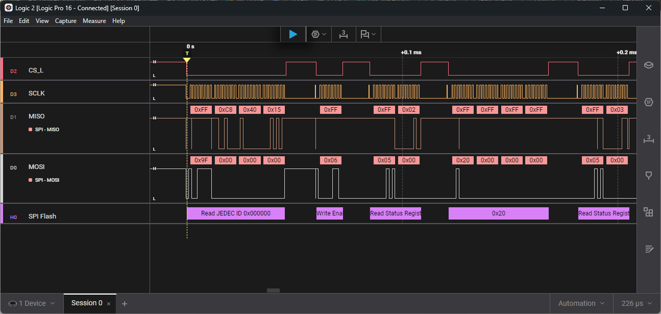
Flash Access - JEDEC ID Read, RSR Read
Keep the first FPGA image deliberately boring
The current gateware is intentionally small. Its top level instantiates generated Git identity logic and a soft SPI register block. There is no fabric clock in this milestone; the register interface is clocked directly from external SPI SCK. That narrows the number of unknowns during bring-up and makes the first successful transaction evidence about the physical interface rather than a large application design.
Each transaction is seven bytes:
an opcode (
0x02for write, or0x03for read),a 16-bit address, and
a 32-bit big-endian value.
The initial register map exposes a magic word, FPGA API version, short Git hash, commit count, 64-bit commit timestamp, build flags, status, and a writable scratch register at address 0x0020.
The first register decoder is deliberately plain Verilog. A function provides the complete read map in one place:
case (address)
    16'h0000: register_value = MAGIC;
    16'h0004: register_value = FPGA_API_VERSION;
    16'h0008: register_value = git_hash_short;
    16'h000C: register_value = git_commit_count;
    16'h0010: register_value = git_commit_time[31:0];
    16'h0014: register_value = git_commit_time[63:32];
    16'h0018: register_value = {31'd0, git_dirty};
    16'h001C: register_value = 32'h00000001;
    16'h0020: register_value = scratch;
    default:  register_value = 32'h00000000;
endcaseSource: register_value() in fpga/rtl/spi_registers.v
MCU-side fpga_reg_read() and fpga_reg_write() construct the same seven-byte frame, while the Python API checks address and value widths before presenting them as CLI commands.
The magic value answers “is anything intelligible on this bus?” The API version answers “can this MCU safely interpret it?” The build fields answer “which HDL source produced the image now running?” The scratch register proves writes as well as reads. A hardware test wrote 0x12345678 to 0x0020 and read the same value back through the complete chain: CLI, USB, MCU parser, SPI master, FPGA RTL, and back again.
$ fnk fpga reg-write 0x0020 0x12345678
ADDR=0x0020 VALUE=0x12345678
$ fnk fpga reg-read 0x0020
ADDR=0x0020 VALUE=0x12345678
The matching simulation sequence is part of tb_spi_registers.v, so the same behavior is checked without hardware on every test run.
Embedding source identity in both MCU firmware and FPGA gateware turns version reporting into part of the interface. It also creates a reproducibility wrinkle: vendor FPGA tools often insert wall-clock timestamps into output headers. Funkshun normalizes Radiant’s timestamp field while retaining Git-derived identity inside the configuration data, making equivalent builds stable without erasing useful provenance.
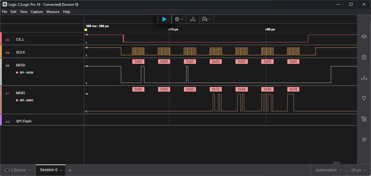
Readback of the scratch register via SPI
Test boundaries, not only functions
The test strategy mirrors the architecture. Python tests cover command construction, fragmented responses, CLI delegation, device discovery, DFU transitions, binary streaming, and identity parsing. Native C tests exercise the MCU line parser, SHA-256, SPI NOR page and sector behavior, update recovery, and flash readback mismatch handling. A Verilog testbench reads identity registers and writes and reads the scratch register. Build scripts also test generated Git metadata and bitstream normalization.
The important cases live at boundaries: a USB packet ending in the middle of a command, a payload containing a newline, a flash page boundary, a transfer abandoned halfway through, a USB identity changing during DFU, or an FPGA that raises CDONE but speaks an incompatible API. Those are the cases most likely to work in a single demonstration and fail later in a product.
The Payoff: application work becomes ordinary register design
With this foundation working, the next Funkshun milestone can finally be about the function generator. DDS phase increments, amplitude, waveform selection, trigger configuration, output enables, and status can become documented FPGA registers. The MCU can provide higher-level commands and policy while the FPGA owns cycle-accurate signal generation.
That division is the real architectural result. USB and updates are not entangled with HDL application logic. The MCU can evolve its user interface without rebuilding the FPGA for every presentation change. The FPGA can add datapath features behind a versioned register map. Both images identify themselves, and either can be updated from the same CLI.
An MCU/FPGA system becomes much easier to develop when the FPGA is not treated as a mysterious peripheral that happens to load at power-up. An explicit boot contract, an electrical ownership protocol, a versioned runtime interface, and a recovery story, all provide the plumbing that makes deployment of new gateware breezily simple. Then the interesting FPGA work can proceed on top of infrastructure that is already observable, testable, and hard to brick.